


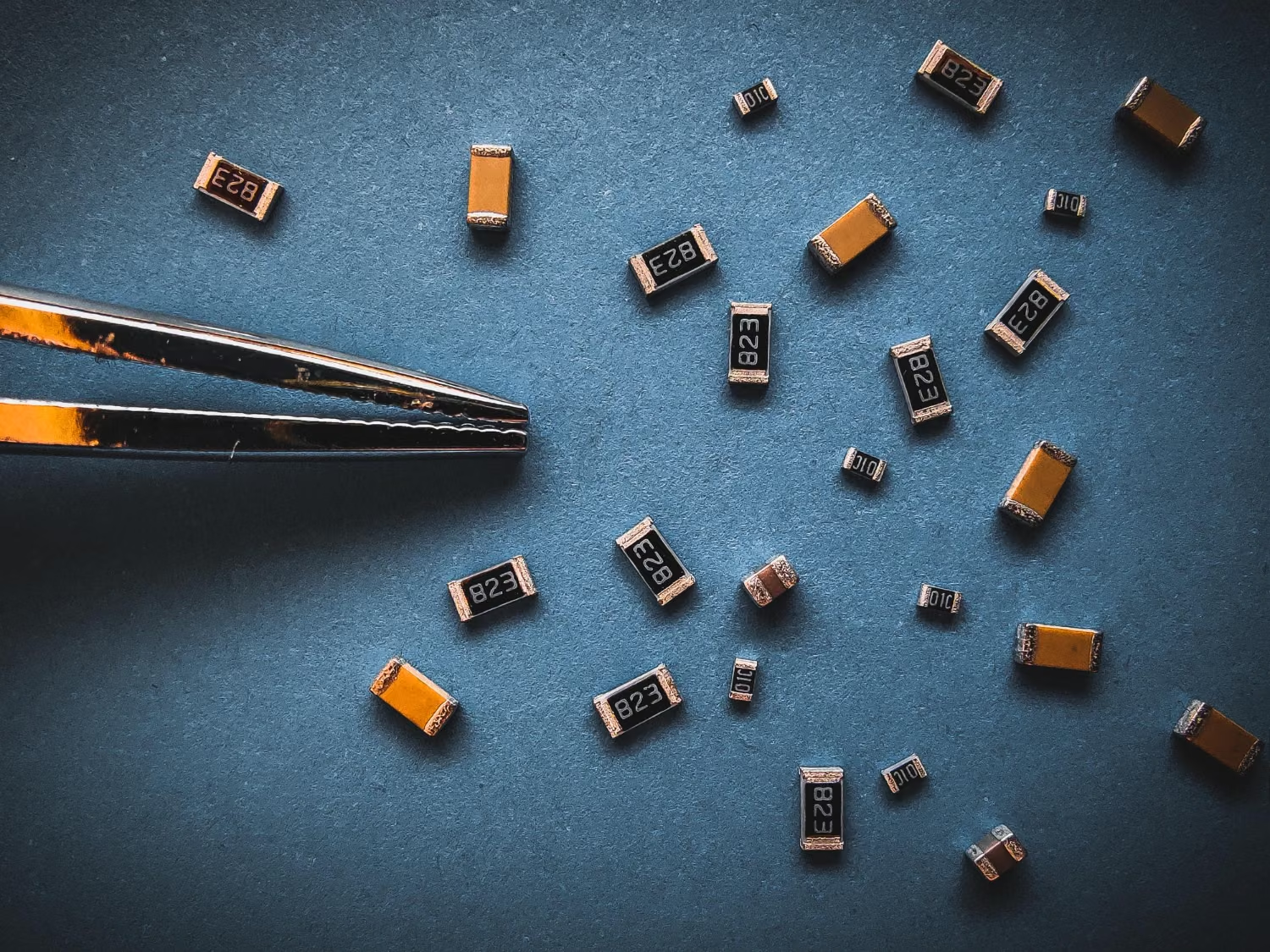
Miniaturisation is an important trend in electronics. Devices can combine more functions in smaller, lighter packages, while new technologies create opportunities to improve energy efficiency. What does this mean for electronics manufacturing?
Why is miniaturisation changing electronics?
Miniaturisation affects industries from automotive and medical equipment to consumer electronics. It creates opportunities in several areas:
- Performance and energy efficiency: New semiconductor and packaging technologies can reduce component size while maintaining or improving functionality. Efficiency gains depend on the design and operating conditions; a smaller device does not automatically consume less power or generate less heat.
- Applications in connected and embedded systems: Smaller integrated circuits help combine functions in compact housings. This supports Internet of Things (IoT) devices, embedded systems and suitable AI applications.
- Precision and reliability in manufacturing: Smaller components require appropriate surface-mount technology (SMT) and inspection methods. Qualified processes help manufacturers assemble compact circuits consistently.
- Production-cost opportunities: Introducing finer assembly processes requires investment. Smaller components may reduce board area and material use, but the total cost also depends on PCB complexity, component prices and manufacturing yield.
- Opportunities for Polish electronics manufacturers: Companies such as Techbit can support compact designs through SMT and through-hole technology (THT) assembly and an agreed inspection and final-integration scope. Each design must be checked against the equipment and process capabilities.
Miniaturisation also brings challenges. Smaller parts and denser layouts require precise assembly and inspection, careful thermal design and attention to electromagnetic compatibility. Manufacturers need to qualify the process rather than assume that reducing size preserves reliability.
From microprocessors to nanoscale technologies
Continued miniaturisation supported the development of personal computers, mobile phones and portable devices. Processor integration increased over successive generations, eventually enabling multicore processors. Another important development was the use of microelectromechanical systems (MEMS) in applications such as motion sensing and navigation.
PCB development also contributed: printed circuit boards increasingly used surface-mount devices (SMDs), allowing denser component layouts.
Modern semiconductor manufacturing has enabled levels of integration that were difficult to imagine decades earlier. Advanced processors can contain billions of transistors and may use process families described as 3 nm. The node name is not a direct measurement of every transistor feature. Developments in FinFET structures, new semiconductor technologies and research into carbon nanotubes continue to explore further improvements in integration, power and performance.
Key technologies supporting miniaturisation
Smaller electronic products rely on advances in manufacturing and materials. Three important areas are SMT assembly, PCB fabrication and semiconductor integration. Each contributes to reducing size while supporting the required functions.
These three areas offer different advantages:
- SMT assembly: allows denser component placement and automated production.
- Advanced PCBs: support more interconnections and greater layout flexibility.
- Integrated semiconductor devices: can combine functions and improve efficiency within the appropriate design.
One important change was the increasing use of SMT alongside traditional through-hole assembly (THT) and the adoption of surface-mount devices (SMDs). Mounting components on board surfaces allows denser layouts and smaller assemblies. THT remains useful where its mechanical or electrical properties suit the application.
Miniaturisation has also increased the use of components that combine functionality with a smaller footprint:
- Highly integrated microcontrollers : combine multiple functions in one device, reducing the need for separate parts.
- Small resistors and capacitors : include SMD packages such as imperial 0201, approximately 0.6 × 0.3 mm.
- Multifunction packages : examples include system-in-package (SiP) devices, which integrate multiple elements in one package and save board space.
Related topic: how does SMD soldering work?
Benefits and challenges of miniaturisation
Compact designs can improve portability and functionality, but may be harder to repair or recycle. The benefits need to be weighed against the full product life cycle.
Reducing board and component size may reduce some material requirements, including:
- Conductive metals such as copper, gold and silver used in interconnections,
- Plastics used in housings and insulation,
- Device weight and volume, potentially reducing transport and storage requirements.
Energy-efficiency improvements may come from new transistor technologies and appropriate circuit design. Advanced process nodes can offer power-efficiency benefits, but the actual result depends on workload, architecture and operating conditions.
Miniaturisation can contribute to lower environmental impacts when it reduces material or energy use. The overall footprint still needs to account for manufacturing, product lifetime and end-of-life treatment.
There are also tradeoffs, particularly in servicing and repair:
- Component integration : system-on-chip (SoC) and system-in-package (SiP) solutions combine functions in a die or package, which can make individual functions harder to replace.
- SMT assembly : components are soldered to the PCB surface. Small parts can require skilled rework and suitable tools rather than being simple to replace manually.
- Smaller connections and solder joints : ball grid array (BGA) packages and very small components may require specialist removal and rework equipment, increasing service costs.
As a result, some devices are difficult or uneconomical to repair, which can contribute to electronic waste and shorter practical product lifetimes. Repairability should be considered during design.