


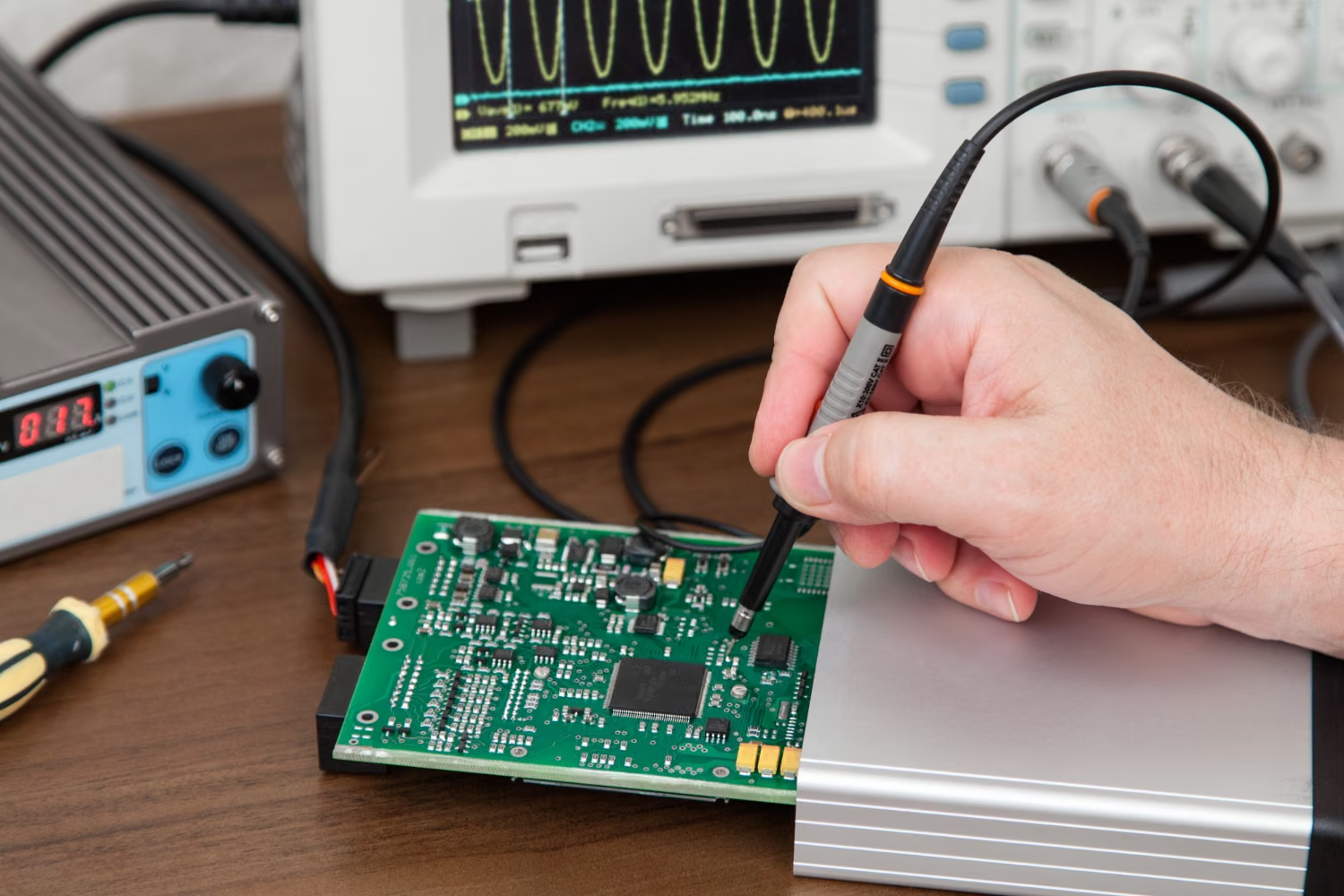
Testing printed circuit boards (PCBs) is part of the life cycle of an electronic product. It covers stages from design and prototyping through production to final checks before a finished device reaches the customer. Each stage helps assess whether the product meets its quality and functional requirements.
Why is PCB testing important?
Testing serves several purposes throughout a product's life cycle:
- Design verification: During design, testing helps engineers check whether the PCB meets the intended functional and technical requirements. Identifying errors early makes it possible to correct them before volume production, reducing rework costs and delays in bringing the product to market.
- Quality control: During production, testing helps check whether each manufactured PCB meets the specified acceptance criteria. Faulty units can then be identified and addressed before they reach the end user.
- Reliability assessment: Final validation can include functional and environmental tests, depending on the product requirements. These assess operation under the conditions for which the device was designed, including moisture, temperature, vibration and other environmental factors.
- Process verification: Production testing also helps monitor and improve the manufacturing process. Analysing the results can reveal where changes are needed, supporting efficiency and reducing waste.
Quality and reliability matter to both manufacturers and end users. PCB testing contributes to both in several ways:
- Improving quality: Thorough, systematic testing helps detect manufacturing defects. Resolving those defects supports product quality, customer satisfaction and confidence in the brand.
- Improving reliability: Environmental and functional testing assess whether a product performs as expected under defined conditions. This is especially relevant in automotive, defence and energy applications where reliable operation is critical.
- Reducing repair and warranty costs: Detecting and correcting defects early reduces the costs associated with later repairs and warranty claims. This supports profitability and protects the manufacturer's reputation.
- Improving safety: Testing helps identify faults that may affect user safety. In safety-critical automotive or defence applications, the test scope must be matched to the product's risks and requirements.
In short, PCB testing supports quality and reliability through design validation, production inspection and final checks. It can contribute to a successful product and more satisfied customers.
Types of inspection and testing
The following methods provide different kinds of evidence about a board. They complement one another; the appropriate combination depends on the design, production volume and acceptance requirements.
Automated optical inspection (AOI)
Automated optical inspection (AOI) is one of Techbit's core PCB inspection methods. We perform AOI off-line, on a separate machine. Cameras and image-analysis software scan the board surface to identify potential assembly and manufacturing defects.
Advantages of AOI:
- Speed and repeatability: automated inspection helps identify visible production defects promptly so they can be reviewed and corrected.
- Detection of different defects: AOI can identify visible solder-joint issues, missing components and incorrect component placement. Coverage depends on visibility and inspection-program settings.
- Reduced manual inspection effort: automation limits repetitive visual checks and helps reduce operator-dependent variation.
In-circuit test (ICT)
In-circuit test (ICT) checks electrical properties of components and connections on an assembled PCB.It can identify electrical and assembly faults within the coverage of the test programme and available test access.
Advantages of ICT:
- Electrical measurements: ICT can measure parameters such as resistance and capacitance, helping assess whether the assembly matches its specifications.
- Assembly-defect detection: it can identify issues such as open circuits, shorts, incorrect component values or faulty connections, depending on coverage.
- Production suitability: ICT can support repeatable series testing. Fixture cost and test-point access must be considered, particularly for prototypes and small batches.
Functional testing
Functional testing checks how a device behaves in defined operating scenarios. At Techbit, the scope is agreed for the project; the customer provides the tester and instructions where applicable. Tests may cover basic functions and more complex operating sequences.
Advantages of functional testing:
- Functional verification: an agreed test sequence checks the specified operations against expected results.
- System-level fault detection: it can reveal problems that are not apparent when individual components are tested separately.
- Representative operating conditions: testing under conditions similar to actual use helps assess the functions and behaviour relevant to the application.
Environmental testing
Environmental testing assesses product operation under specified environmental conditions. It can include temperature, humidity, vibration and other factors that may influence performance.
Advantages of environmental testing:
- Reliability assessment: testing under demanding conditions can expose weaknesses that should be addressed before release.
- Environmental protection: the results help assess measures intended to protect electronics against moisture, dust and other harmful factors.
- Standards and qualification: tests conducted to applicable procedures can provide evidence for product qualification. Required facilities, standards and certification routes must be established separately.
Common faults and their causes
PCB testing can reveal faults that affect functionality and reliability. Common examples include:
Poor or cold solder joints, which may result from inadequate heating, unsuitable soldering parameters, contaminated surfaces or an inappropriate flux process. These can create weak or unreliable electrical connections.
Solder bridges, where excess solder forms an unintended connection between adjacent pads or component leads. Contributing factors include excessive solder deposition and insufficient spacing.
Missing components caused by assembly errors, such as incorrect feeding or placement by assembly equipment.
Components can also be damaged during transport, storage or assembly, or may arrive with manufacturing defects.
PCB testing therefore serves both to identify problems and to assess whether finished products meet the specified quality, safety and reliability requirements.At Techbit, the agreed inspection and test plan supports defect detection before delivery. No single test method can establish that every possible fault is absent.
Impedance: what is it and why does it matter?
Impedance describes the opposition to alternating current (AC) in an electrical circuit. It matters in PCB design and testing, particularly for high-speed, radio-frequency (RF) and microwave circuits. Impedance mismatches can cause reflections, interference and signal loss. They can also reduce power transfer and efficiency in RF systems.
PCB testing supports project success
PCB inspection and testing are fundamental parts of electronics manufacturing. Available industry methods include AOI, X-ray inspection, ICT, functional testing and environmental testing. Each provides different coverage. For your project, agree the methods, equipment, acceptance criteria and responsibilities before production begins.