


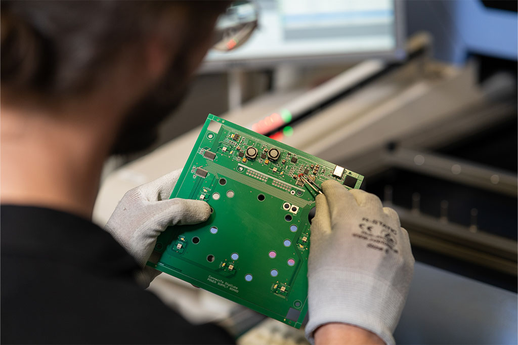
Are you unsure what a PCB is or how to select one for electronics production? This article explains its role, common constructions and the practical points to discuss with a manufacturer.
What is a printed circuit board?
A printed circuit board (PCB) mechanically supports electronic components and provides conductive connections between them. Boards range from simple single-layer constructions to multilayer stack-ups with insulating material separating copper layers.
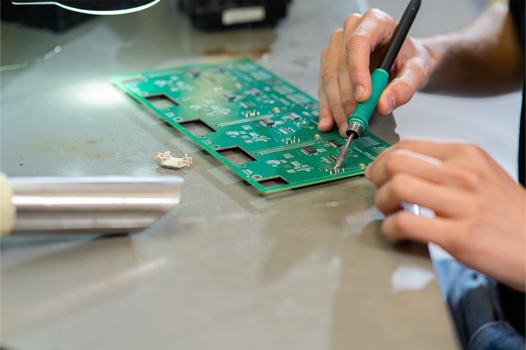
Copper tracks, pads and vias form the connections required by the circuit design. Components such as resistors, capacitors and integrated circuits are mounted and soldered to create a printed circuit board assembly (PCBA).
What does PCB stand for?
PCB stands for printed circuit board. It is a widely used foundation for electronic devices and systems.
What does a PCB do?
A PCB serves several important functions:
- It supports components and connects them to carry electrical power, data and signals.
- Its layout allows components and connections to be organised within limited space. Protection against shorts, surges and electromagnetic interference requires appropriate circuit and layout design; the board alone does not provide it automatically.
- Compared with hand-wired assemblies, a PCB can use space efficiently and support repeatable production. Design revisions are implemented through updated board documentation and fabrication rather than rewiring each unit.
Where are PCBs used?
Ten examples include:
- Consumer electronics: televisions, phones, laptops, printers and many other everyday products.
- Industry: production-machine controls, process-control systems and quality-monitoring equipment.
- Automotive electronics: systems such as audio, navigation and climate control.
- Communications: routers, modems and cable or satellite equipment.
- Energy: power supplies, uninterruptible power systems and voltage converters.
- Medical equipment: devices such as defibrillators and electrocardiogram monitors, with application-specific safety and qualification requirements.
- Space applications: satellite and launch-vehicle electronics, subject to demanding qualification requirements.
- Defence electronics: control, radar and communications systems.
- Building automation: lighting, heating and ventilation controls.
- Industrial electronics: manufacturing control and inspection systems.
Common PCB types
PCB constructions can be classified in several ways:
- Single-sided PCB: has one conductive copper layer. Component placement depends on whether the design uses through-hole or surface-mount assembly.
- Double-sided PCB : has conductive layers on both faces, with connections between them where required. Components may be placed on one or both sides.
- Multilayer PCB : combines several conductive layers separated by dielectric material, with suitable vias connecting the required layers.
- Flexible PCB: uses a flexible substrate to accommodate a defined shape or bend.
- Hybrid PCB: combines different substrate materials or technologies where the application requires them. Mechanical fasteners alone do not define a board as hybrid.
- Metal-core PCB : includes a metal base, commonly aluminium, to support heat transfer in a suitable construction.
- High-density interconnect (HDI) PCB : uses features such as fine conductors and microvias to create more interconnections in a limited area.
What are PCBs made from?
Common substrates include glass-reinforced epoxy materials such as FR-4 and paper-based phenolic laminates. Flexible and high-frequency boards use other materials suited to their requirements. Material selection affects electrical, thermal and mechanical behaviour.
PCB fabrication
The exact process depends on the construction, but common stages include:
- Preparing copper-clad material and panels according to the intended board construction.
- For multilayer boards, patterned layers are combined with dielectric materials and laminated. Board thickness and stack-up are design parameters agreed with the fabricator rather than fixed universal limits.
- Applying a photosensitive resist to define the required copper pattern.
- Exposing and developing the resist so the intended tracks and pads are represented.
- Etching unwanted copper, with other operations such as drilling and plating incorporated as required by the construction.
- Applying appropriate solder mask and surface finish, then completing fabrication and inspection. These coatings have specific functions and should not be confused with conformal coating applied to an assembled board.
What defines a suitable PCB?
A suitable board meets the documented electrical, mechanical and manufacturing requirements:
- The substrate and construction must be appropriate for the operating environment.
- The conductors and interconnections must implement the design accurately.
- Thermal requirements should be addressed through the stack-up, copper, heat-transfer paths and relevant system design.
- Some designs use embedded passives, blind or buried vias, or differential-pair routing. These are application-specific features rather than requirements for every high-quality board.
- Electrical testing, using flying probes or a fixture as appropriate, helps check bare-board continuity and isolation against the netlist. It does not establish every aspect of finished-device functionality.
Analysing PCB faults and defects
Different methods provide different information:
- Visual inspection can identify physical damage, visible solder issues or loose components on an assembly.
- An oscilloscope or logic analyser can examine signals and reveal unexpected behaviour during circuit operation.
- X-ray inspection can help assess hidden structures or connections where appropriate.
- Specialist methods, including thermal imaging, acoustic techniques or 3D X-ray analysis, may be selected according to the suspected fault and the investigation requirements.
Why PCBs matter to the electronics industry
PCBs support interconnection in products ranging from phones and computers to medical equipment and industrial robots. Their different shapes, sizes and constructions allow the board to be matched to the application.
From layout development to component assembly, the PCB provides a defined platform for implementing a circuit.
Repeatable board manufacture also supports prototyping and design revisions. Its value depends on accurate documentation, suitable materials and fabrication against the specified requirements.
How should you select a PCB for production?
Selecting a board construction can be complex. Discuss it with the design team, fabricator and assembly partner. Confirm materials, stack-up, dimensions, finishes, tolerances and inspection requirements before ordering.
- At Techbit, quantities and sourcing are discussed around the project, whether you need a prototype for testing or a repeatable production batch.
- Multilayer-board sourcing and assembly must be checked against the documented construction and process capabilities. We do not assume that every technical parameter can be accepted without review.
- Before assembly, we review documentation and manufacturability requirements. Design for manufacturing (DFM) concerns production feasibility, while IPC-A-610 addresses acceptance of electronic assemblies; it is not a bare-board design standard.
- Storage of boards for later assembly orders can be agreed as part of the project. Stock availability, storage conditions and the production schedule need confirmation rather than an assumption of immediate assembly.
Conclusion
A PCB is a small but important part of an electronic product. Choosing it requires careful assessment and, where needed, advice from the relevant specialists. Would you like to discuss your assembly requirements?
Contact Techbit to review board sourcing, assembly, inspection and any agreed storage arrangements for your project: Electronics manufacturer Techbit